nanofab@diaotuotech.com
+86-19820819249
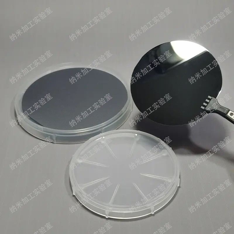
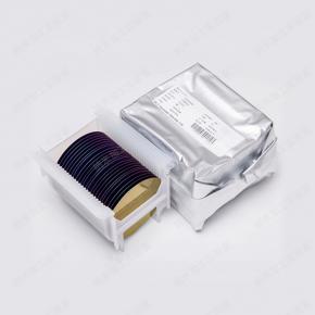
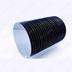
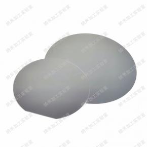
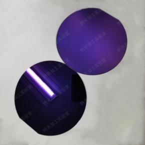
Silicon Wafer——FZ Silicon Wafer (Domestic)
Product description:
Silicon wafer——FZ silicon wafer (domestic)
1. Doping type: N, P
2. Diameter: 2~8 inches
3. Resistance value: tens of Ωcm-20kΩcm and above
4. FZ silicon wafer refers to the silicon wafer made by the zone melting method. The silicon rod is melted from one end of the seed crystal, and the melting zone is gradually moved to the other end of the silicon rod. Using the segregation principle and evaporation characteristics of impurities, the silicon The rods are purified and a very uniform impurity distribution is obtained. This technique is usually used to manufacture high-purity intrinsic silicon wafers.
5. Whether to do high-temperature process, and the process performance after annealing are an important index for investigating FZ silicon wafers.
6. According to the process application, different types of FZ silicon wafers are applicable. When consulting, you need to inform the process application and whether to do high-temperature process.
Contact: Mike
Phone: +86-19820819249
Tel: +86-19820819249
Email: nanofab@diaotuotech.com
Add: Room 103, Building P, Navigator Sci-Tech Park, No. 163, Banxuegang Avenue, Bantian Street, Longgang District, Shenzhen City, Guangdong Province, P.R. China
We chat