nanofab@diaotuotech.com
+86-19820819249
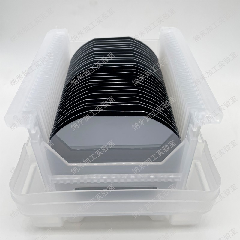
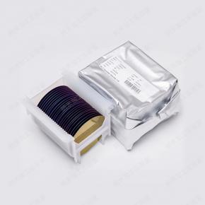
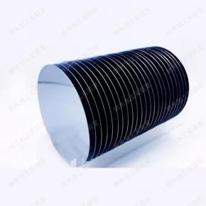
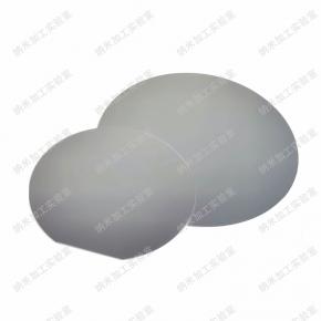
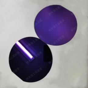
Silicon Wafer - SOI Silicon Wafer
Product description:
Silicon Wafer - SOI Silicon Wafer
1. Diameter: 4~8 inches
2. Bonding process SOI and Smart cut process SOI can be provided
3. The thickness of the device layer can be as thin as 150nm, and the thickness of the buried oxide layer can be as thin as 1um
4. SOI silicon wafer is silicon on insulating substrate. This technology introduces a buried oxide layer between the top silicon and the back substrate. It can be customized according to the parameters of the device layer, buried oxide layer, and bulk silicon material required by the user, as well as the customization of multi-layer SOI
Contact: Mike
Phone: +86-19820819249
Tel: +86-19820819249
Email: nanofab@diaotuotech.com
Add: Room 103, Building P, Navigator Sci-Tech Park, No. 163, Banxuegang Avenue, Bantian Street, Longgang District, Shenzhen City, Guangdong Province, P.R. China
We chat