nanofab@diaotuotech.com
+86-19820819249
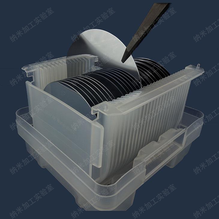
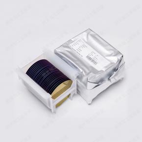
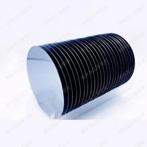
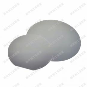
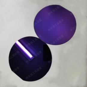
Silicon Wafer - Epitaxial Wafer
Product description:
Silicon Wafer - Epitaxial Wafer
1. Diameter: 2~8 inches
2. Growth of a homogeneous or heterogeneous thin film layer on a single crystal substrate.
3. The new single crystal layer grown by epitaxial growth can be different from the substrate in terms of conductivity type, resistivity, etc., and multilayer single crystals with different thicknesses and different requirements can also be grown.
4. This type of silicon wafer needs to be customized by the user to provide detailed indicators
Contact: Mike
Phone: +86-19820819249
Tel: +86-19820819249
Email: nanofab@diaotuotech.com
Add: Room 103, Building P, Navigator Sci-Tech Park, No. 163, Banxuegang Avenue, Bantian Street, Longgang District, Shenzhen City, Guangdong Province, P.R. China
We chat