nanofab@diaotuotech.com
+86-19820819249
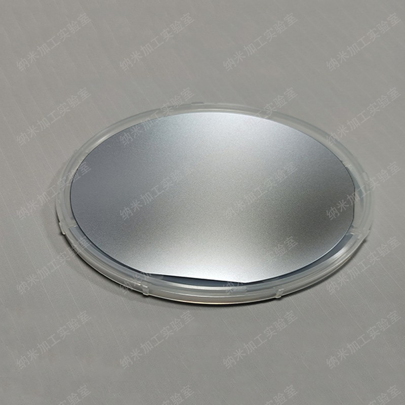
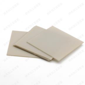
Gallium Arsenide Chip
Substrate - Gallium Arsenide Wafer
1. Diameter: 2~6 inches
2. Crystal orientation: <100>
3. Gallium arsenide sheets are widely used to make integrated circuit substrates, infrared detectors, gamma photon detectors, etc.
4. Various types of III-V substrates can be provided, such as InP, InAs, GaN, GaSb, etc.
Contact: Mike
Phone: +86-19820819249
Tel: +86-19820819249
Email: nanofab@diaotuotech.com
Add: Room 103, Building P, Navigator Sci-Tech Park, No. 163, Banxuegang Avenue, Bantian Street, Longgang District, Shenzhen City, Guangdong Province, P.R. China
We chat