
nanofab@diaotuotech.com
+86-19820819249
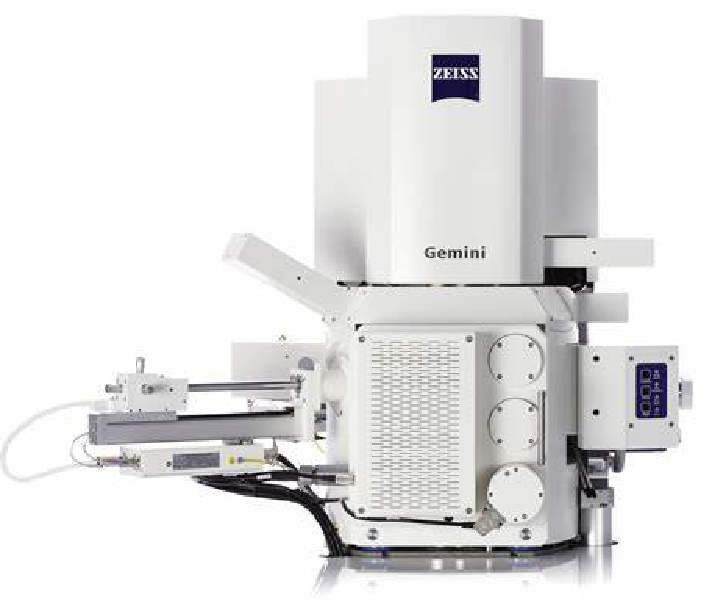
Scanning electron microscope
Type: GeminiSEM300
Manufacturer: Carl Zeiss (England)
Maximum field of view: 50 mm
Maximum sample size: 250 mm in diameter, 50 mm in height
Accelerating voltage: 0.02 kV-30 kV
Magnification: 12 times-2 million times
Secondary electron resolution: ≤0.7 nm@15 kV, ≤ 1.2 nm@30 kV
Sample movement range: X axis: 130 mm; Y axis: 130 mm; Z axis: 50 mm
Maximum sample tilt angle: 70° Maximum electron beam displacement: 200 μm
InLense SE: High-resolution secondary electron detector, which can be used for high-resolution morphology observation;
ET-SE: Secondary electron detector in the sample chamber, which can be used to observe the structure of the microscopic area of the sample surface;
aBSD: The drawable six in the sample chamber Segmented backscattered electron detector, which can be used for sample composition contrast observation;
Oxford Energy Spectrometer System (EDX): can analyze the energy spectrum to obtain the element composition and content of the sample;
Cathodoluminescence spectrometer (CL): excitation wavelength is 270-900 nm, carry out qualitative and quantitative research on the luminescence properties of materials
Contact: Mike
Phone: +86-19820819249
Tel: +86-19820819249
Email: nanofab@diaotuotech.com
Add: Room 103, Building P, Navigator Sci-Tech Park, No. 163, Banxuegang Avenue, Bantian Street, Longgang District, Shenzhen City, Guangdong Province, P.R. China
We chat