
nanofab@diaotuotech.com
+86-19820819249
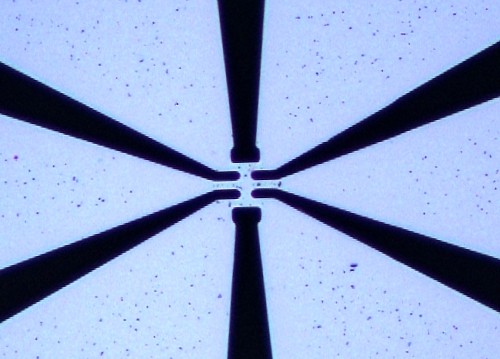
Process introduction:
High-precision silicon-based masks form fine patterns on silicon substrates through micro-nano etching technology and are used for electrical and optoelectronic research on two-dimensional materials. In-situ chips use this mask to deposit metal on thin film materials to create precise metal electrodes.
Product application:
Researchers use silicon-based masks to prepare high-precision two-dimensional material metal electrodes to conduct research on electrical and optoelectronic properties.
Process capabilities:
Minimum line width: 2um
The thinnest non-hollow pattern: 200um
The thinnest hollow pattern: 20um
Contact: Mike
Phone: +86-19820819249
Tel: +86-19820819249
Email: nanofab@diaotuotech.com
Add: Room 103, Building P, Navigator Sci-Tech Park, No. 163, Banxuegang Avenue, Bantian Street, Longgang District, Shenzhen City, Guangdong Province, P.R. China
We chat