
nanofab@diaotuotech.com
+86-19820819249
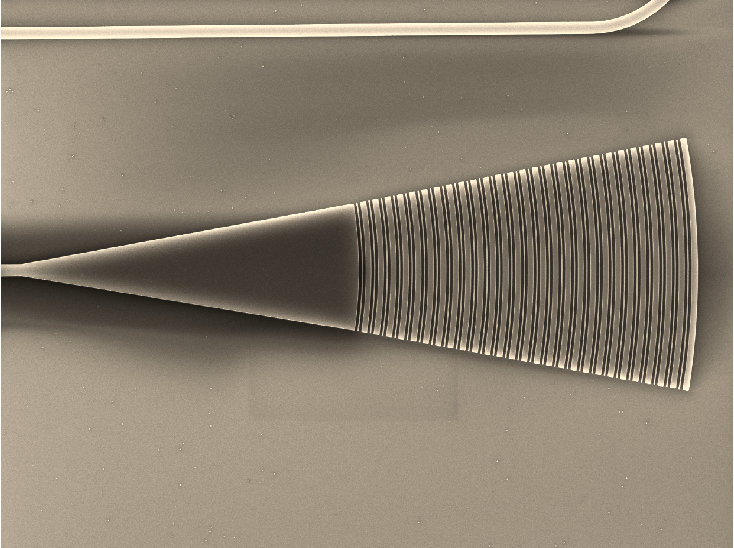
Introduction to the process of optical waveguide devices:
Optical waveguide devices are manufactured on silicon-based or other transparent materials through precision photolithography and etching processes for efficient transmission and control of optical signals.
Process capability:
Materials: silicon, quartz, polymers, etc.
Structural design: Design the waveguide cross-section and refractive index distribution.
Manufacturing: Photolithography defines patterns and etching forms waveguides.
Function:
Transmission: Transmitting optical signals in fiber optic communication.
Modulation: Adjusting the phase or intensity of light waves.
Beam splitting: Splitting an optical signal into multiple paths.
Coupling: coupling optical signals between different waveguides.
Optical waveguide devices are widely used in fields such as integrated optics, optical communication, and sensors.
Contact: Mike
Phone: +86-19820819249
Tel: +86-19820819249
Email: nanofab@diaotuotech.com
Add: Room 103, Building P, Navigator Sci-Tech Park, No. 163, Banxuegang Avenue, Bantian Street, Longgang District, Shenzhen City, Guangdong Province, P.R. China
We chat