nanofab@diaotuotech.com
+86-19820819249
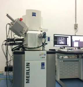
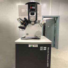
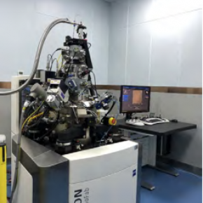
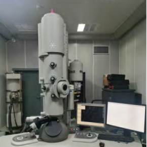
The field emission scanning electron microscope scans the sample with the focused high-energy electron beam to excite various physical information, and realizes the characterization of the sample by receiving, amplifying and displaying the information. The scanning electron microscope can achieve a resolution of 0.8 nm at 15 kV; it is equipped with a secondary electron detector to analyze the surface morphology of the sample, a backscatter detector to analyze the sample composition, a energy spectrometercollecting the X-ray to analyze sample composition, a spectrometer to measure the wavelength for sample composition analysis and an Electron Backscattered Diffraction (EBSD) instrument to analyze the crystal orientation of the sample.
Contact: Mike
Phone: +86-19820819249
Tel: +86-19820819249
Email: nanofab@diaotuotech.com
Add: Room 103, Building P, Navigator Sci-Tech Park, No. 163, Banxuegang Avenue, Bantian Street, Longgang District, Shenzhen City, Guangdong Province, P.R. China
We chat